


In-depth analysis: why network transformers can act as "scavengers" for signal transmission
In the information age, network communication technology is changing with each passing day, and high-speed and stable data transmission has become a key factor in the development of enterprises. As an indispensable component in communication equipment, network transformers play a vital role. Today, VOOHU will give you a comprehensive introduction to the basic concepts of network transformers, how to select them, and their design and application, so that everyone can have a more comprehensive understanding of network transformer products. Welcome to discuss any deficiencies!
1. Overview of network transformers
Network transformers are electronic components specially used in the field of network communications. They are also key components for connecting Ethernet to terminal interfaces. They are responsible for multiple missions such as signal transmission, impedance matching, noise suppression, and high-voltage isolation. They play an indispensable role in the field of communications to ensure the stability and security of data during transmission. The core components of network transformers include magnetic cores, coils, and skeletons. Its working principle is based on electromagnetic induction. The signal received by the primary coil generates a changing magnetic field in the magnetic core, and then induces a voltage in the secondary coil to complete the signal transmission.
Of course, in theory, Ethernet can be directly connected to the terminal interface, but the interference of external circuits and the limitation of transmission distance make this solution a bottleneck in practical applications. The intervention of network transformers, with its unique winding structure-the combination of differential mode inductors and common mode inductors, effectively suppresses the interference of common mode and differential mode signals, realizes signal filtering and enhancement, and thus significantly improves the signal transmission distance. In addition, the application of network transformers also builds an effective isolation barrier between Ethernet and external circuits, greatly enhancing the system's anti-interference ability. Even when facing different voltage connections, the stable operation of Ethernet itself can be ensured. At the same time, the network transformer also provides a certain degree of lightning protection for the equipment.
2. Network transformer components and working principle
The three basic parts of a network transformer are: T (Transformer), K (Common mode Choke), and A (Center Tapped Auto-Transformer). According to different combinations, network transformers are divided into: single T-piece network transformer, T + K-piece network transformer, T + three-wire loop K-piece network transformer, and T + K + A-piece network transformer.
1. Single T-piece network transformer
As shown in the figure below. It is a schematic diagram of a single T-piece network transformer and its ability to prevent EMI from being transmitted to the PHY chip and data signal transmission.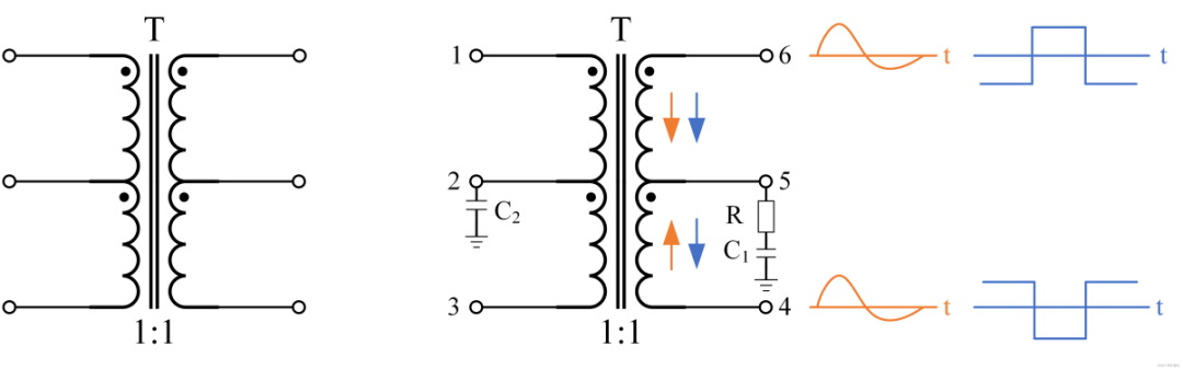
|
Single T-piece network transformer and signal transmission schematic
|
The EMI interference line number (orange signal) on Pin4 and Pin6 is equal in magnitude, opposite in direction, and has exactly the same waveform. The currents they cause in the upper and lower coils of the secondary are equal in magnitude and opposite in direction, canceling each other out. The flux changes caused by the two currents in the magnetic ring cancel each other out. The flux change is zero, which means that the inductive reactance presented by the upper and lower coils of the secondary is zero, and they can be replaced by two short-circuit lines. EMI passes through two short-circuit lines. The middle tap and R-C series circuit discharge EMI to the ground wire, thereby reducing the amplitude of EMI.
For the same reason, EMI from the internal circuit will be discharged to the ground wire through the middle tap and C2 of the primary coil, which can reduce the amplitude of EMI inside the device emitted into the air through the wire.
The blue signal is the data voltage signal. The currents caused in the upper and lower coils of the secondary are equal in magnitude and direction, and the flux changes caused inside the secondary coil of the T-piece are superimposed on each other, showing high inductive reactance.
It can be seen that the network transformer with a middle tap has the function of blocking the mutual propagation of EMI between its primary and secondary coils.
2. T-piece + K-piece network transformer
The schematic diagram of the T-piece + K-piece network transformer and the schematic diagram of signal transmission are shown in the figure below.
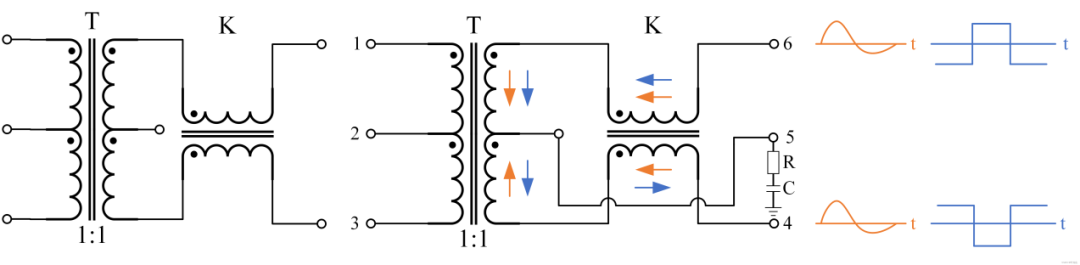
Figure 1 shows the schematic diagram of a network transformer composed of T and K (choke). K is added to the network transformer because it has no attenuation effect on the useful data voltage (differential) signal, but can attenuate EMI. Adding K can further block EMI from propagating between the primary and secondary coils.
As shown on the right side of the above figure, the orange signal is EMI and the blue signal is the voltage differential signal; the orange and blue arrows represent the current direction of EMI and data voltage signals in the primary coils of K and T, respectively. Analysis shows that when the data voltage signal flows from Pin4 and Pin6 through the upper and lower coils of K, the currents are equal in magnitude and opposite in direction. The magnetic flux changes caused by them inside the magnetic ring of K cancel each other out. The magnetic flux change is zero, which means that the inductive reactance presented by the upper and lower coils of K is zero. In other words, without considering the influence of the internal resistance of K, K has no attenuation ability for the data voltage signal.
As shown by the orange arrows in the figure above, when EMI flows through the upper and lower coils of the K-component, the currents generated are equal in magnitude and direction. The changes in magnetic flux caused by them inside the magnetic ring of the K-component are superimposed on each other. The inductive reactance ZL presented by the K-component will increase linearly with the increase of frequency according to the following formula. L is the inductance of the K-component.
ZL=2πfL
The K-component is connected in series in the EMI loop. Before the EMI reaches the secondary coil of the T-component, a considerable part of it will fall on both ends of the K-component, so the choke plays the role of blocking EMI. The K-component has a better blocking effect on the high-frequency components of EMI, because the higher the frequency, the greater the EMI dropped on both ends of the K-component. By the same token, the K-component can also block the EMI generated inside the equipment from being transmitted to the wire. The T-component + K-component network transformer has a further improved EMI attenuation capability compared to the T-component network transformer.
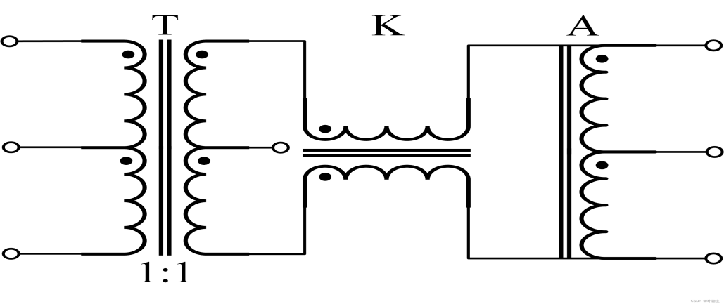
3. T+K+A network transformer Figure 1 below is a schematic diagram of a T+K+A network transformer consisting of T, K and A (autotransformer). The inductance of the newly added A in the figure is relatively large, usually 1.5~2.0mH. The reason why A is added to the network transformer is that the added A with a large inductance does not significantly attenuate the useful data voltage signal, but can further block the propagation of EMI between the primary and secondary sides of the transformer.
|
Figure 1 Schematic diagram of T+K+A network transformer
|
The schematic diagram of the network transformer transmitting data voltage signal and EMI is shown in Figure 2. In the figure, the blue signal is the data voltage signal, the orange signal is the EMI; the orange arrow and the blue arrow are the directions of the current of the data voltage signal and the EMI signal in the network transformer respectively.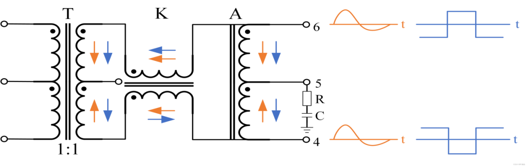
|
Figure 2 Schematic diagram of signal transmission of T+K+A network transformer
|
As can be seen from the figure, when EMI passes through the upper and lower coils of the autotransformer, their directions are opposite, and the changes in magnetic flux caused by them inside the magnetic ring of part A cancel each other out, so the inductive reactance presented by part A is close to zero, and EMI is discharged to the ground through the R-C series circuit, thereby reducing the amplitude of EMI. The discharge effect of part A is similar to that of the secondary coil of part T. When the data voltage signal passes through the upper and lower coils of the autotransformer, its direction is the same, and the changes in magnetic flux caused by them inside the magnetic ring of part A are superimposed on each other, so the inductive reactance presented by part A is very large.
EMI is triple-processed by part A (autotransformer), part K (choke) and part T secondary coil, which greatly reduces the amplitude of EMI, and the attenuation ability of the network transformer to EMI is greatly improved.
| Note: The K and A components in the network transformer can further curb the propagation of EMI generated inside and outside in the network port communication circuit, but they also have a certain negative impact on the normal data signal, because both the K and A components have parasitic and distributed parameters. For example, there is line capacitance between the two coils of the K and A components, and these capacitors are connected in parallel at both ends of Pin6 and Pin4. Connecting capacitors in parallel at the output or input end of the network transformer will inevitably compress the frequency band at its high-frequency end. The narrowing of the frequency band will slow down the rising front edge and falling back edge of the data voltage signal passing through it, resulting in a decrease in the data transmission rate. Therefore, it is sufficient to arrange one K and one A component in the network transformer, or to arrange one K component on the primary side and secondary side of its T component. If the number of K or A components is increased, it will not only increase the production cost, but also reduce the data transmission rate. Since the secondary coil of the T component plays the role of the A component, the most commonly used network transformer is the one composed of the T component and the K component. |
3. Classification of network transformers
Network transformers are mainly classified based on the following core parameters: structure type, packaging type, transmission rate, number of ports, application environment, and POE power supply capacity
1. Classification based on structure type:
RJ45 connectors of separate network transformers and integrated network transformer modules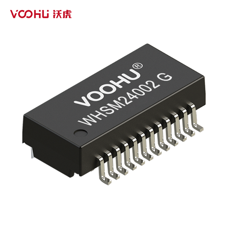
| WHSG24002G | SYT-320DBL |
| Single-port Gigabit network transformer | RJ45 integrated Gigabit transformer |
2. Classification by package type:
SMD surface mount
DIP plug-in perforation
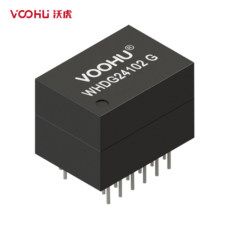
| WHSG24002G | WHDG24102G |
| Single-port Gigabit SMD network transformer | Single-port Gigabit plug-in network transformer |
3. Classification by transmission rate:
10/100 Base-TX
Gigabit Base-TX
2.5G Base-T
5G Base-T
10G Base-T
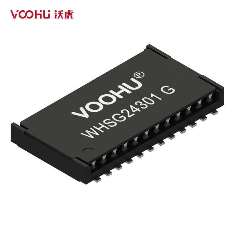
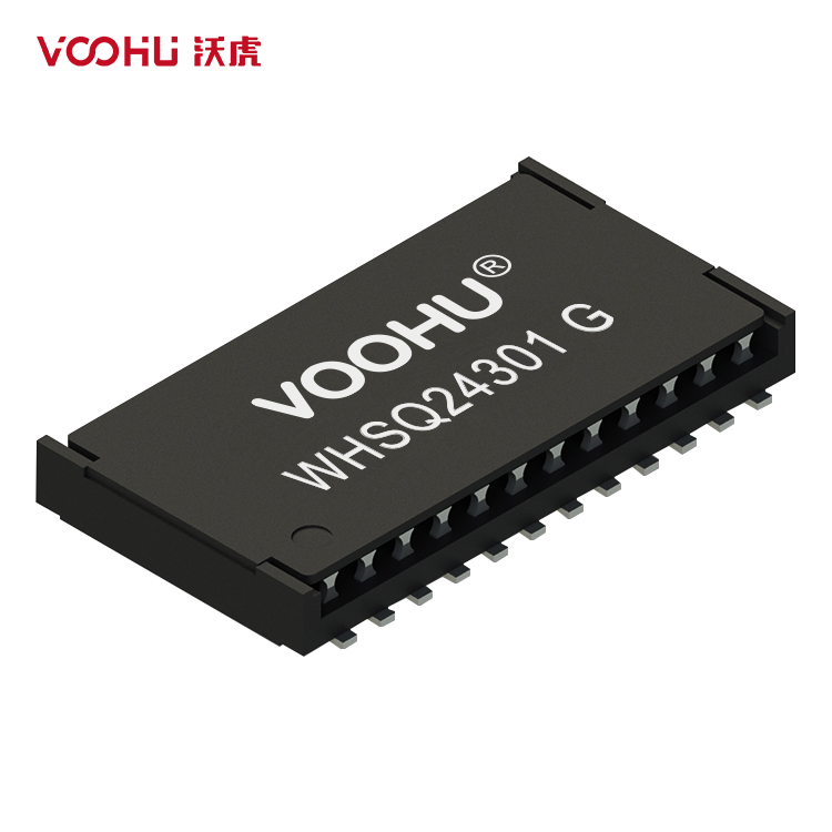

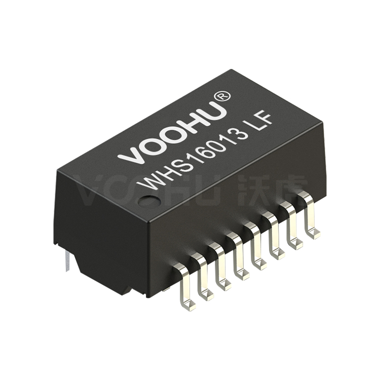
| WHS16013LF | WHSG24301G | WHSQ24301G | WHSM24002G |
| 100M | Gigabit | 2.5G/5G | 10GNetwork transformer |
| Network transformer | Network transformer | Network transformer |
4. Classification by number of ports:
Single Port
Dual Ports
Quad Ports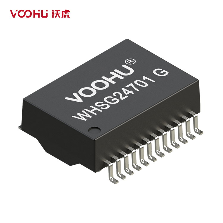
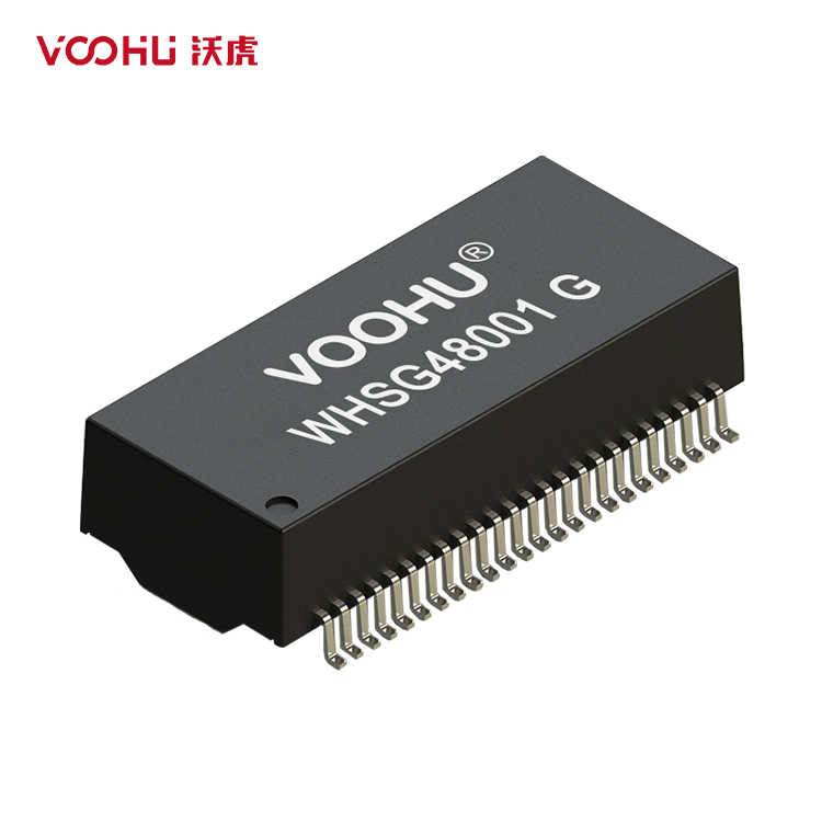
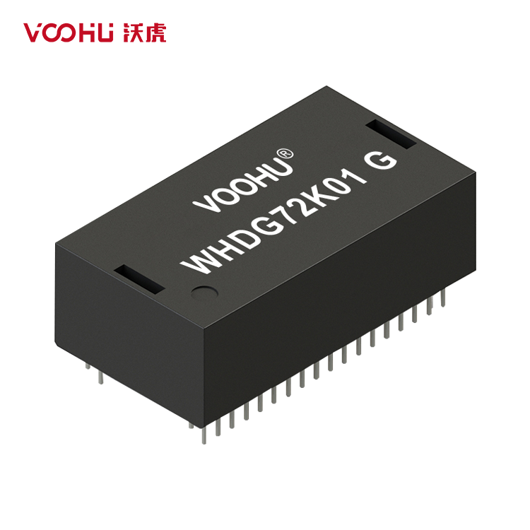
| WHSG24701G | WHSG48001G | WHDG72K01G |
| Single-port Gigabit | Dual-port Gigabit | Four Gigabit ports |
| Network transformer | Network transformer | Network transformer |
5. Classification based on the operating temperature of the customer's application environment:
Consumer Electronics (Consumer Operation Temp.: 0~70°C)
Industrial Equipment (Industry Operation Temp.: -40~+85°C)
Automotive (Automotive Operation Temp.: -40~+125°C)
Military and Aerospace (Mili-Aero Operation Temp.: -55~+155°C)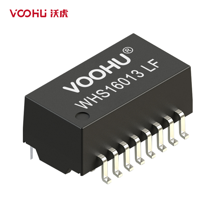
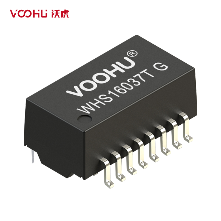
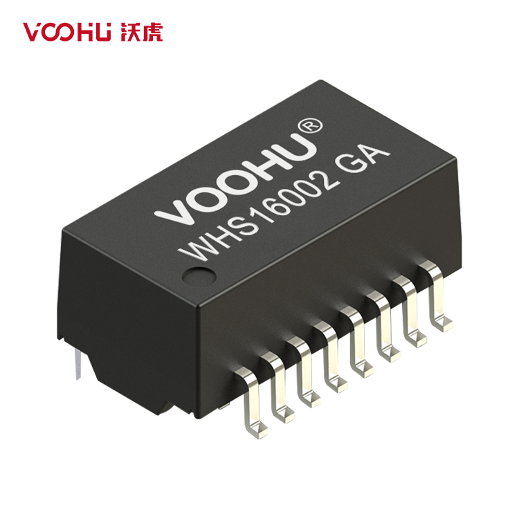

| WHS16013LF | WHS16037TG | WHS16002GA | WHS16002GM |
| (Consumer grade) | (Industrial Grade) | (Automotive Grade) | (Military Grade) |
6. Classification based on POE power supply capacity:
Non-PoE
(Meets IEEE802.3ab Standard)
PoE
(15W power supply capacity,
Meets IEEE802.3af Standard)
PoE+
(30W and above power supply capacity,
Meets IEEE802.3at Standard)
4PPoE
(90W power supply capacity,
Meets IEEE802.3bt Standard)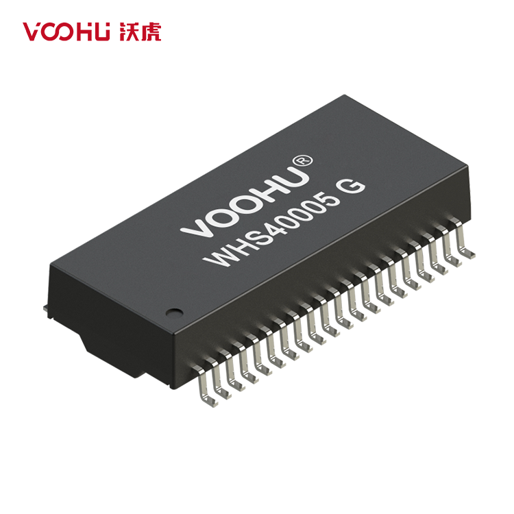

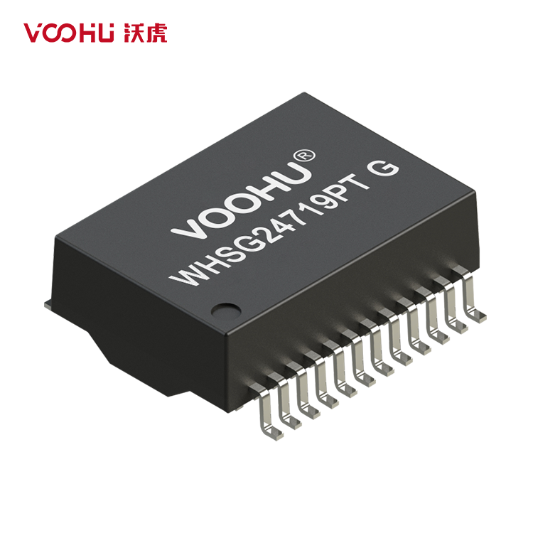
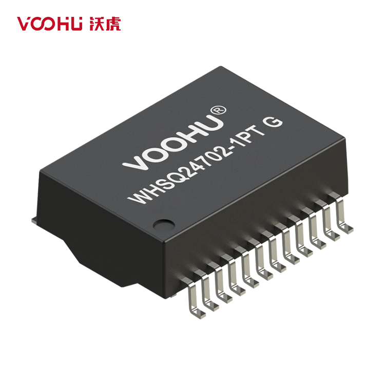
| WHS40005G | WHSG24015G | WHSG24719PTG | WHSQ24702-1PTG |
| Four 100M ports | Single-port Gigabit | Single-port Gigabit | 2.5G/5G |
| Non-POE | POE:15W | POE:30W | POE:90W |
4. Design and selection of network transformers
PHY chips are divided into voltage-type PHY and current-type PHY according to the interface driver type. In the actual networking process, the local device cannot predict the type and level requirements of the other device, but due to the existence of the transformer, the interconnection of different types of PHY chips only needs to refer to the strategies of different level AC coupling, that is, just take care of their own local matching. When both sides are voltage-type PHY, since the interface of voltage-type PHY is standard, there is no problem in interconnecting through the transformer, and the center tap of the transformer can be directly grounded through a capacitor; when both sides are current-type PHY, since the interface driver of current-type PHY requires current injection, the center tap of the transformer needs to be connected to the power supply, and the pull-up voltage depends on the common-mode voltage required by the PHY chip itself; when the voltage-type PHY and the current-type PHY are connected, the pull-up power supply of the taps on both sides can be based on the requirements of their respective PHY chips, even if they are different, it does not matter, because the transformer cannot transmit DC voltage.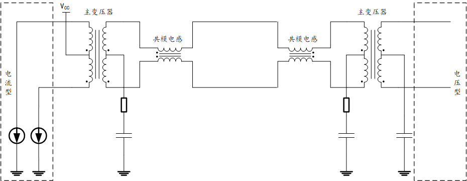
|
Figure 1 Interconnection between voltage-based PHY and current-based PHY
|
Common-mode inductors are divided into two types: two-wire common-mode and three-wire common-mode. They can be placed on the PHY side, the cable side, or both sides. Several placement methods are shown in Figure 1.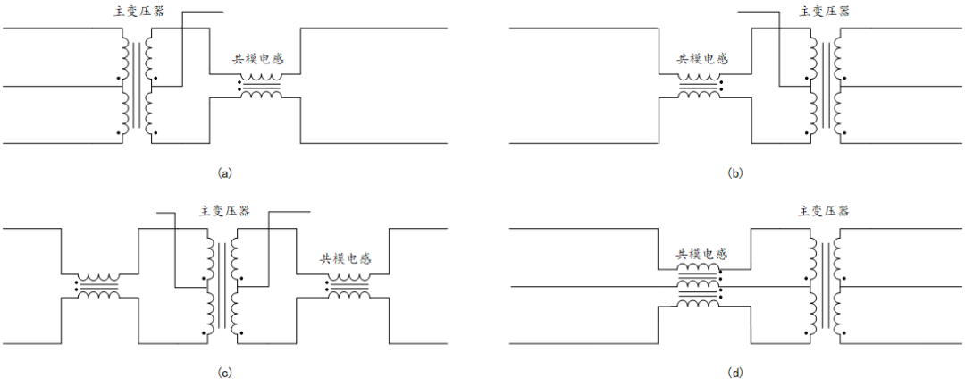
|
Figure 2 Schematic diagram of common mode inductor placement
|
Placing the common-mode inductor on the cable side can better filter the interference caused by transformer imbalance, which is an advantage compared to placing it on the PHY side. However, in the POE power supply scenario, the common-mode inductor on the PHY side does not need to bear the POE current and is not easy to saturate, so its size can be made smaller, which is more beneficial in layout, and its EMC performance is also better. Since the current-type PHY requires an external power supply to provide current, when used with a two-wire common-mode inductor, when the output is low, the current passes through the main transformer and the upper half of the common-mode inductor to form a loop, and vice versa when the output is high. When the output is 0, the current passes through the two coils of the common-mode inductor to form a loop. When the current flows through only one coil, the magnetic field generated cannot be offset, and the common-mode inductor exhibits high impedance, which affects the signal quality of the normal signal. When using a three-wire common mode, no matter what current is output, the current will flow through the two coils in opposite directions, and the magnetic fields will cancel each other out, which has no effect on the signal.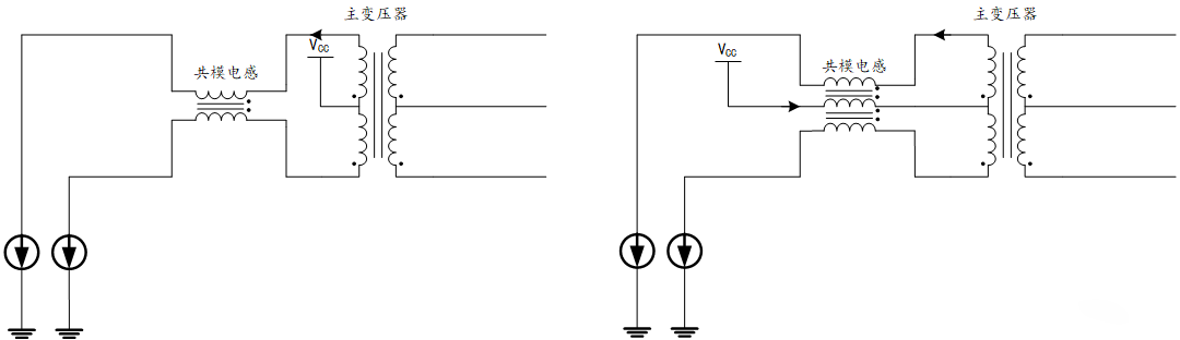
|
Figure 3 Two-wire common mode and three-wire common mode inductors with current-mode PHY
|
If the requirements for relevant EMC indicators are high, the structure shown in Figure 1 (c) will be adopted, and common-mode inductors will be arranged on both the PHY side and the cable side. In order to adapt to current-type PHY, the common-mode inductor on the PHY side can be changed to a three-wire common mode. In summary, in scenarios where POE power supply is not required, the compatibility and benefits of the two-wire common-mode inductor and the cable side placement solution are higher, but in the POE scenario, the three-wire common mode and PHY side placement solution can be given priority.
Based on the above analysis, the following table is compiled for reference when selecting an Ethernet transformer: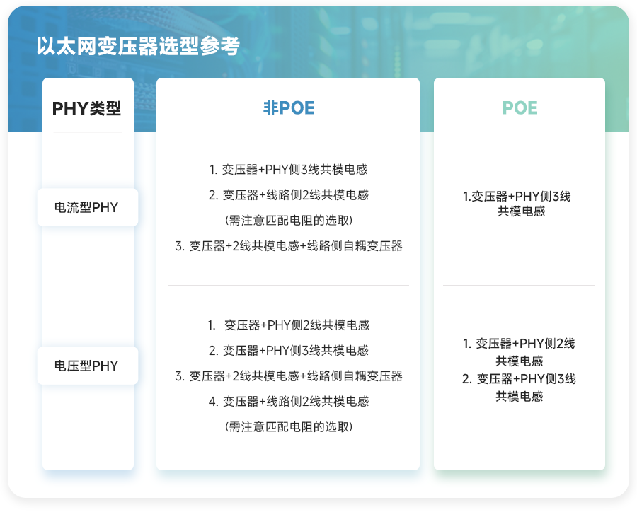
VOOHU can provide customers with comprehensive selection needs.
1. If you need electronic files or paper selection materials, you can leave us a message in the background. Or follow the official account: VOOHU Electronics
2. Enter our website: https://www.voohu.cn to select the model. Our platform supports selection parameters, data download and small batch purchase of samples. Strongly recommended
3. Send your needs to our sales and customer service staff, and we will recommend conventional materials for you to choose. Customer service hotline: 400-1048-018
5. Network transformer design and application
1. Separate network transformer application:
Figure 1 below is a typical application of Ethernet. Our PCB design is basically laid out and wired according to this block diagram. Below we will use this block diagram to explain the layout and wiring points related to Ethernet.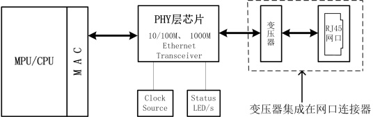
|
Figure 1 Reference circuit where the Ethernet port transformer is not integrated into the Ethernet port connector
|
PCB layout and wiring diagram. The following uses Figure 2 to introduce the key points that need to be paid attention to in the layout and wiring of the Ethernet circuit.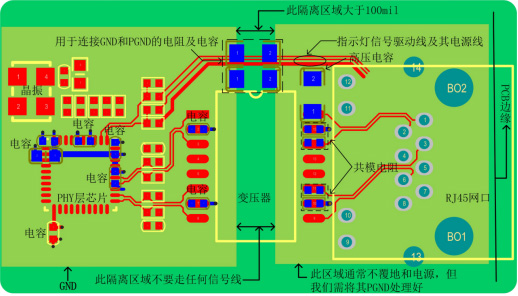
|
Figure 2 PCB layout and wiring reference for the circuit where the transformer is not integrated into the network port connector
|
2. Transformer-separated RJ45 design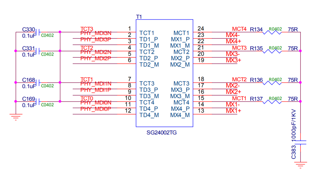
|
Non-integrated RJ45 interface
|
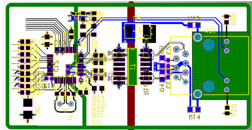
3. PCB layout requirements
1) When the transformer and RJ45 interface are separated, as shown in the figure, the distance between the RJ45 interface and the transformer should be shortened as much as possible (while meeting the process requirements)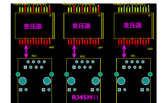
2) The distance between the Ethernet conversion chip PHY and the transformer should also be as short as possible, generally not exceeding 5 inches. If the RJ45 interface comes with a transformer, the Ethernet conversion chip should be placed as close to the RJ45 interface as possible, as shown in the figure below.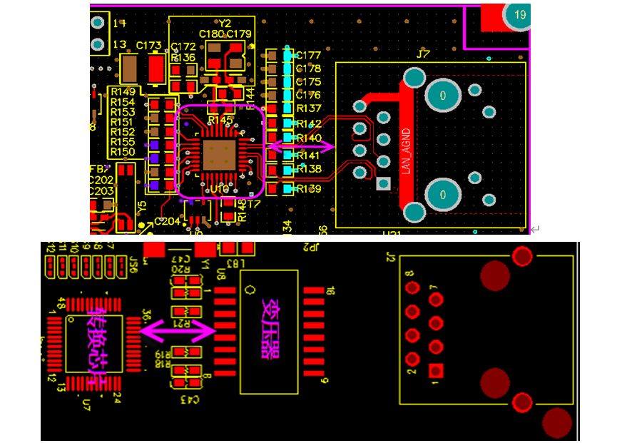
3) As shown in the figure below, the placement of the AC termination resistor is generally based on the chip manual recommendations. Some chips require placement at the Ethernet converter end. If there are no special requirements, place it close to the Ethernet conversion chip.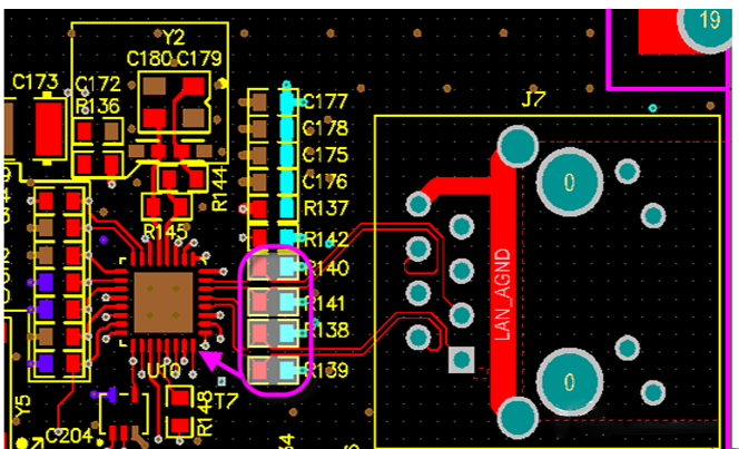
4) The reset circuit signal should be as close to the Ethernet conversion chip as possible, and if possible, should be away from the TX+/-, RX+/- differential signals and clock signals;
5) The clock circuit should be as close to the Ethernet conversion chip as possible, away from the edge of the circuit board and other high-frequency signals, IO port routing and other magnetic components;
According to the above layout requirements, the overall layout diagram can be summarized as shown in the following figure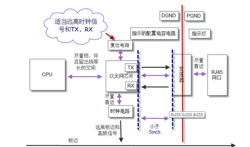
|
RJ45 layout overview
|
4. PCB wiring requirements
1) TX+, TX- and RX+, RX- should be placed on the surface as much as possible. The spacing between the two differential pairs should be at least 4w, and the equal length constraint within the pair is 5mil. The two differential pairs do not need to be equal in length, as shown in Figure 1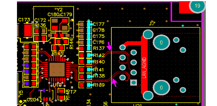
|
Figure 1 RX, TX differential wiring requirements
|
2) Considering that the transformer is an interference source, all layers below the transformer need to be hollowed out. It is only necessary to hollow out the silk screen of the transformer without digging out the pads, as shown in Figure 2.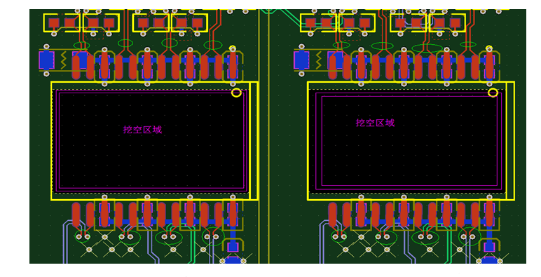
|
Figure 2: Hollowing out the bottom of the transformer body
|
3) The transmission part from PHY chip to CPU (GTX_CLK\TX_EN\TX_ER\TXD[7:0]) and the receiving part (GRX_CLK\RX_DV\RX_ER\RXD[7:0]) should be routed separately. Do not mix the receiving and transmitting networks. The distance between the lines should meet 3W. RX and TX should be of equal length, within 100mil, and the impedance should be controlled to 50 ohms.
4) The routing of power signals, including the routing of decoupling capacitors, power lines, and ground lines should be kept short and wide. The diameter of the vias on the decoupling capacitors should be slightly larger. Each capacitor should have an independent via to the ground, and the ground via should not be shared;
5) AC termination generally needs to be connected to the chip or transformer after passing through a resistor. No STUB lines are allowed;
6) For the differential pairs of Gigabit Ethernet, the optimal signal layer should be selected for routing. The number of vias should not exceed two, and when punching holes to change layers, return ground vias should be added within 200mil, as shown in Figure 3.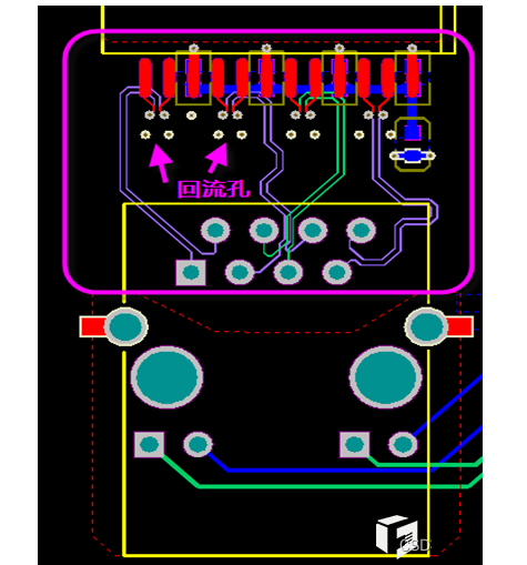
|
Figure 3 Placement of reflux holes
|
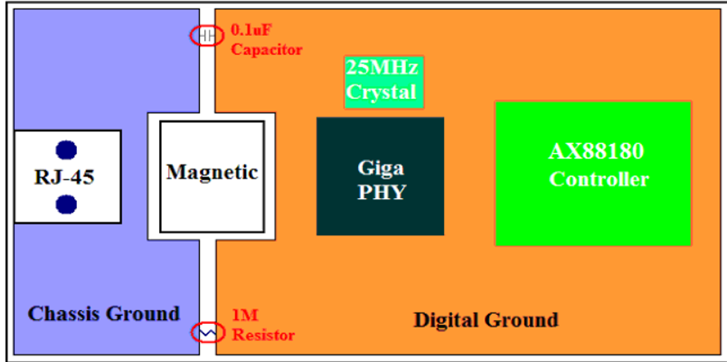
7) Principles of power and ground processing: The RJ45 chassis ground and digital ground are isolated by a 1M ohm resistor and a 0.1uF decoupling capacitor. The spacing between the chassis ground and the digital ground must be wider than 60mil, as shown in Figure 4 and Figure 5.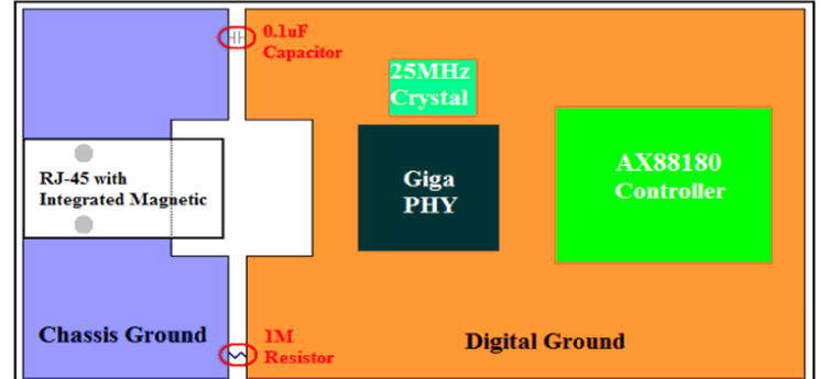
|
Figure 4 Typical transformer integrated single RJ45 chassis/digital ground plane
|
|
Figure 5 Typical RJ45 and transformer separated chassis/digital ground plane
|
All digital and analog power planes with different supply voltages should be isolated, as shown in Figure 6 and Figure 7.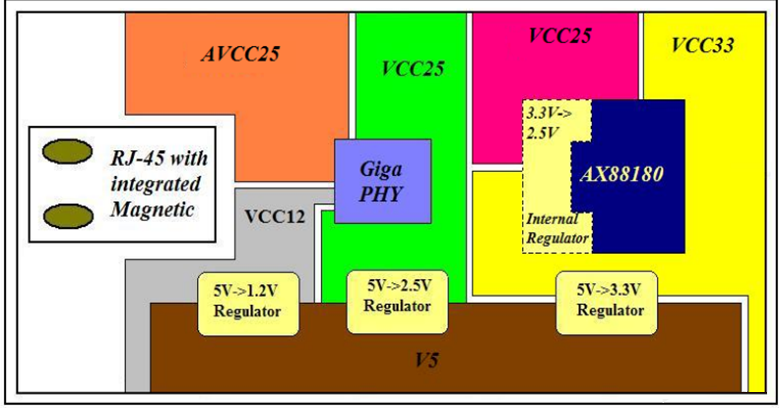
|
Figure 6 Typical transformer integrated single RJ45 digital/analog power plane
|
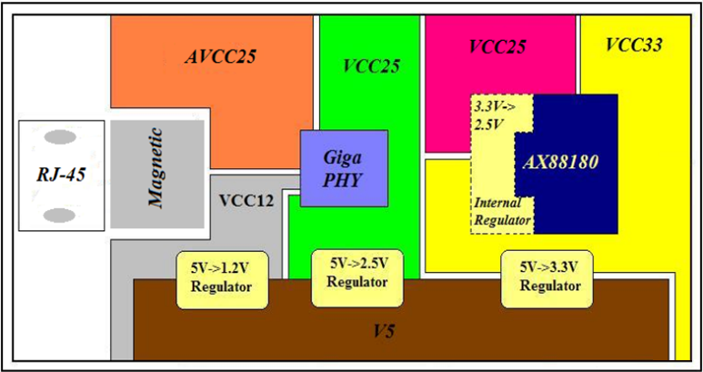
| Figure 7 Typical RJ45 and transformer-independent digital/analog power planes |
| Note: When the signal from the Ethernet physical layer interface device is connected to the RJ45 network port socket, it is necessary to pay attention to the following: the metal casing and the metal front panel connected to the printed circuit board should be isolated from the internal circuit of the printed circuit board (including the signal and ground layer) by at least 5mm. The ground of the electrostatic current discharge path of the printed circuit board should give priority to the casing ground. The metal parts and metal connectors on the board should be connected to the casing if they can be connected to the casing. If they cannot be connected to the casing, they should be connected to the electrostatic protection ground ring or the working ground. The working ground should be a large-area ground formation. |
Newsletter subscription
Subscribe to our newsletter and stay updated on the latest information of our company and product.
Name
|
I agree that the information that I provide will be used in accordance with the terms of Voohu International Inc. Privacy & Cookies Policy


