


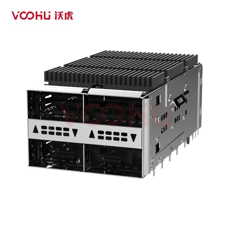
EMI Shielding Design for SFP Cages: How to Reduce Electromagnetic Interference?
EMI Shielding Design for SFP Cages: How to Reduce Electromagnetic Interference?
In high-speed communication systems, electromagnetic interference (EMI) is one of the key challenges that affect signal integrity and device stability. As the core carrier of optical modules, the shielding design of the SFP (Small Form-factor Pluggable) cage directly determines its anti-interference ability. Especially in high-frequency application scenarios such as 5G and data centers, how to optimize the EMI shielding performance of the SFP cage has become a top priority in the design of communication connectors.
01 Why does the SFP cage need precision shielding?
As the interface between the optical module and the device motherboard, the SFP cage needs to deal with two types of interference risks during high-frequency signal transmission:
1. Internal interference: The electromagnetic waves generated by the optical module when working leak through the cage gaps and interfere with other components;
2. External interference: External electromagnetic noise invades through the interface, resulting in an increase in the signal bit error rate.
If the shielding effectiveness is insufficient, it may cause signal attenuation at best, or even cause system downtime. According to the IEC 61967 standard, communication equipment must pass the radiated emission test in the 30MHz-6GHz frequency band, which places strict requirements on the shielding design of the SFP cage.
02 Five core elements of SFP cage EMI shielding design
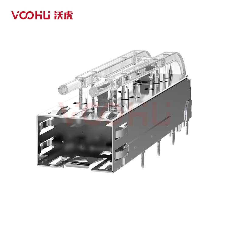
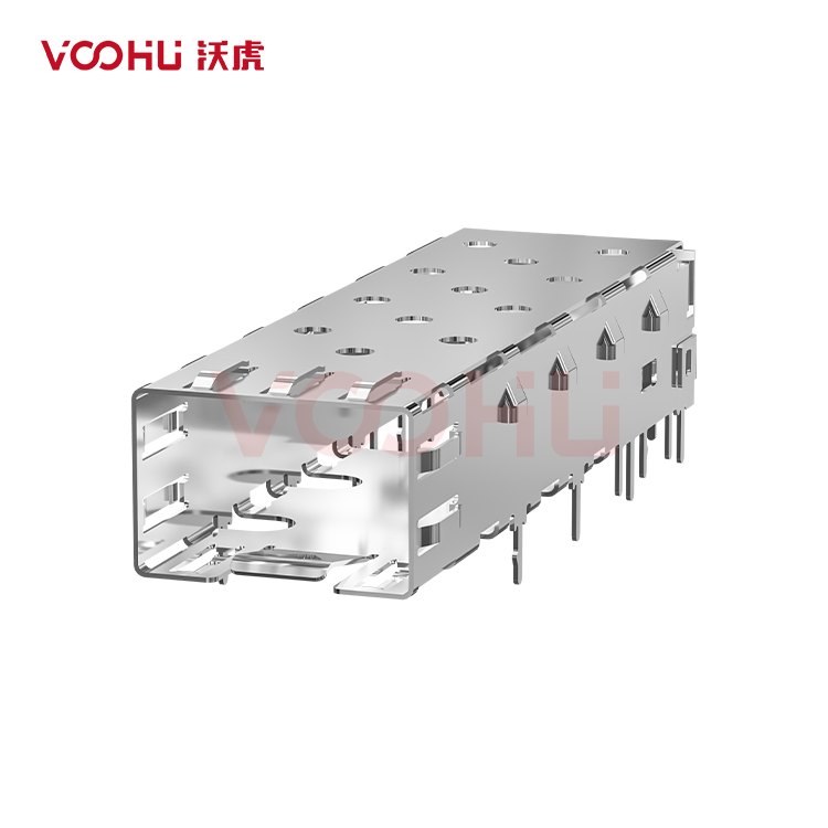
1.Selection of high conductivity materials
Base material is preferably made of high conductivity metals such as stainless steel (SUS304) or beryllium copper (C17200) to ensure that electromagnetic waves form eddy current losses on the surface of the shield;
Surface treatment: gold plating (0.1-0.2μm) or nickel plating (3-5μm) to reduce contact impedance and enhance high-frequency shielding effectiveness (SE≥60dB@1GHz).
2.Integrated fully enclosed structure design
Hole size control: heat dissipation holes and assembly holes must follow the λ/20 principle (aperture < 1/20 of the highest frequency wavelength). For example, the aperture corresponding to 6GHz must be less than 2.5mm;
Sealing of shielding cover: Seamless crimping between the cover and the cage is achieved through spring sheets or conductive foam, and the gap width is controlled within 0.1mm.
3.Multi-point grounding and low impedance paths
Spring contact design: elastic contact points (≥4 points/surface) are set on both sides of the cage to ensure reliable connection with the PCB ground layer (contact resistance <10mΩ);
Ground pad optimization: Use a "well"-shaped or grid-shaped pad layout to shorten the ground path and reduce the return impedance.
4.Avoid cavity resonance effect
Structural simulation assistance: Use ANSYS HFSS or CST software to simulate the cavity resonant frequency, adjust the length-to-width ratio of the cage, and avoid the operating frequency band (such as 3.5GHz for 5G);
Absorbent material filling: Ferrite coating is applied to non-critical areas to absorb stray electromagnetic waves in specific frequency bands.
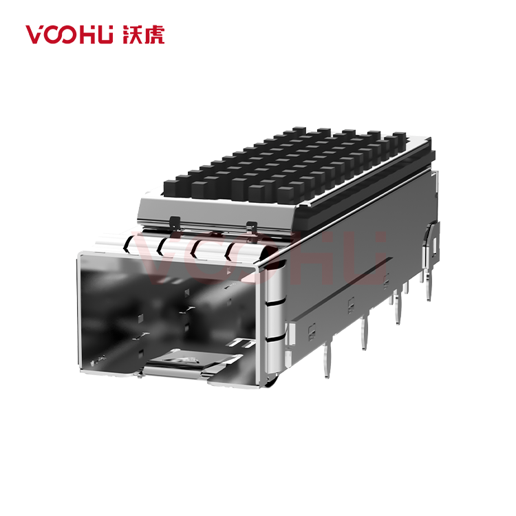
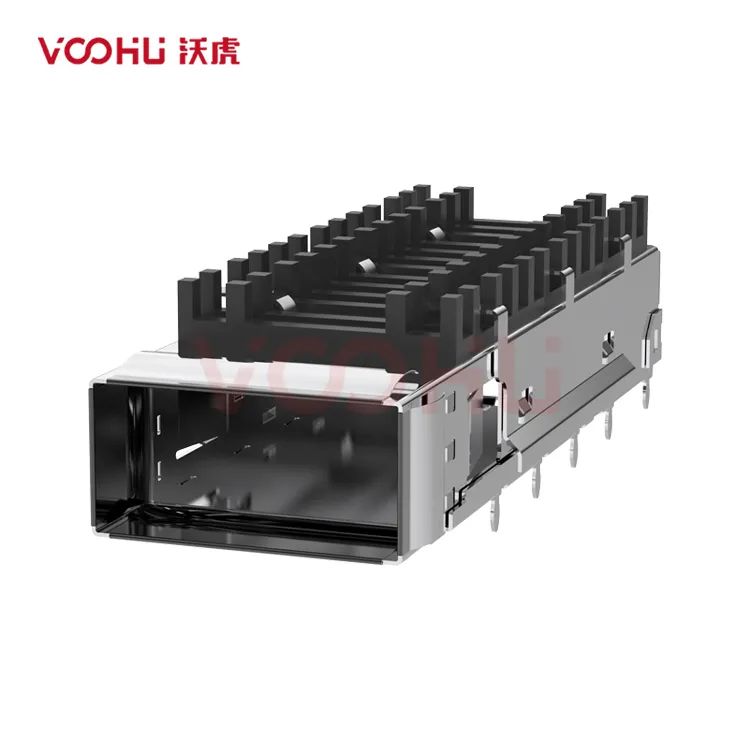
5.Balance between heat dissipation and shielding
Directional heat conduction design: Add a thermal conductive silicone pad on the inside of the shielding cover to direct the heat to the device shell to avoid weakening the shielding performance due to too many openings;
Material composite technology: metal-plastic integrated molding (LDS technology) is used to embed insulating materials in local non-shielded areas to reduce thermal coupling interference.
03 Industry Trends: Future Innovation Directions of Shielding Technology
1.New composite materials: graphene coatings and metallized ceramics in the ultra-high frequency band;
2.Intelligent shielding: active noise suppression technology with integrated EMI sensors;
3.Miniaturization process: MIM (metal injection molding) process to achieve complex cavity structure.
Follow [voohu Electronics] to get EMI test reports and samples!
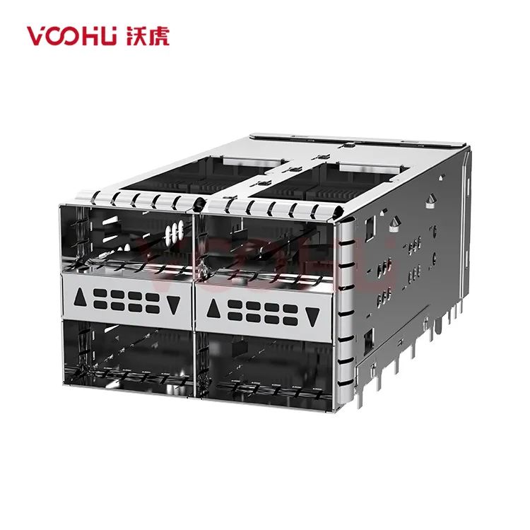
01 Why does the SFP cage need precision shielding?
As the interface between the optical module and the device motherboard, the SFP cage needs to deal with two types of interference risks during high-frequency signal transmission:
1. Internal interference: The electromagnetic waves generated by the optical module when working leak through the cage gaps and interfere with other components;
2. External interference: External electromagnetic noise invades through the interface, resulting in an increase in the signal bit error rate.
If the shielding effectiveness is insufficient, it may cause signal attenuation at best, or even cause system downtime. According to the IEC 61967 standard, communication equipment must pass the radiated emission test in the 30MHz-6GHz frequency band, which places strict requirements on the shielding design of the SFP cage.
02 Five core elements of SFP cage EMI shielding design
1.Selection of high conductivity materials
Base material is preferably made of high conductivity metals such as stainless steel (SUS304) or beryllium copper (C17200) to ensure that electromagnetic waves form eddy current losses on the surface of the shield;
Surface treatment: gold plating (0.1-0.2μm) or nickel plating (3-5μm) to reduce contact impedance and enhance high-frequency shielding effectiveness (SE≥60dB@1GHz).
2.Integrated fully enclosed structure design
Hole size control: heat dissipation holes and assembly holes must follow the λ/20 principle (aperture < 1/20 of the highest frequency wavelength). For example, the aperture corresponding to 6GHz must be less than 2.5mm;
Sealing of shielding cover: Seamless crimping between the cover and the cage is achieved through spring sheets or conductive foam, and the gap width is controlled within 0.1mm.
3.Multi-point grounding and low impedance paths
Spring contact design: elastic contact points (≥4 points/surface) are set on both sides of the cage to ensure reliable connection with the PCB ground layer (contact resistance <10mΩ);
Ground pad optimization: Use a "well"-shaped or grid-shaped pad layout to shorten the ground path and reduce the return impedance.
4.Avoid cavity resonance effect
Structural simulation assistance: Use ANSYS HFSS or CST software to simulate the cavity resonant frequency, adjust the length-to-width ratio of the cage, and avoid the operating frequency band (such as 3.5GHz for 5G);
Absorbent material filling: Ferrite coating is applied to non-critical areas to absorb stray electromagnetic waves in specific frequency bands.
5.Balance between heat dissipation and shielding
Directional heat conduction design: Add a thermal conductive silicone pad on the inside of the shielding cover to direct the heat to the device shell to avoid weakening the shielding performance due to too many openings;
Material composite technology: metal-plastic integrated molding (LDS technology) is used to embed insulating materials in local non-shielded areas to reduce thermal coupling interference.
03 Industry Trends: Future Innovation Directions of Shielding Technology
1.New composite materials: graphene coatings and metallized ceramics in the ultra-high frequency band;
2.Intelligent shielding: active noise suppression technology with integrated EMI sensors;
3.Miniaturization process: MIM (metal injection molding) process to achieve complex cavity structure.
Follow [voohu Electronics] to get EMI test reports and samples!
share to
Related links
You may also like
Prev article
Next article
Newsletter subscription
Subscribe to our newsletter and stay updated on the latest information of our company and product.
Name
|
Subscribe
I agree that the information that I provide will be used in accordance with the terms of Voohu International Inc. Privacy & Cookies Policy


